Intro
The need for accurate timing of clock signals has become very essential in recent time due to their use in varieties of electronic designs . The successful realization of many digital circuits critically depends on the accurate timing of clock signals, which is the base clock that controls the operation of all other components in that device.
Different types of timer IC are being used to realize timed clock signals in systems, each with its associated characteristics.
The type of timer IC adopted by designers depends on a set of requirements for
a given system.
The features of a NE555 timer that makes it adorable for this
design are presented below:
·
precise timing From Microseconds to Hours,
·
adjustable Duty Cycle,
·
Astable or Monostable Operation, and
·
TTL-Compatible Output.
This
project will adopt a 555 timer operating at Astable mode to realise a modest 1s
(one second) clock pulses that will serve well as a time control signal for the
implementation of a high precision digital clock circuits.
The design
The schematic of the 555 timer operating at Astable mode is
shown below in figure 1.
Figure 1: Standard NE555 Astable Circuit
Time/Frequency Calculation
Careful selection of Ra, Rb and C
values will determine the output frequency of the timer.
NOTE: The tolerance of the resistors and capacitors used will slightly affect the desired output frequency. For high end results, high precision components are recommended to be used.
NOTE: The tolerance of the resistors and capacitors used will slightly affect the desired output frequency. For high end results, high precision components are recommended to be used.
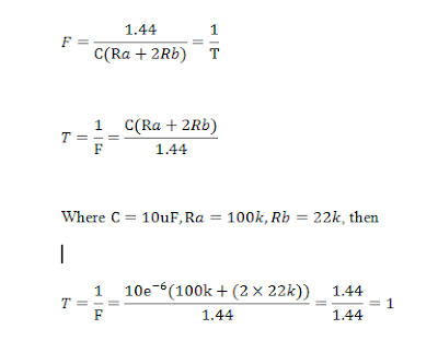
The formula and the required calculation to realise 1 second
astable signal are given below;
See video of the design result: 1 seconds clock
-<|====Watch
Duty Cycle (Mark/Space ratio or High/Low ratio) Calculation
Note: To achieve duty cycle less than 50%, a diode can be connected in parallel to resistor Rb with the negative/cathode terminal of the diode pointing towards the capacitor. This bypasses Rb during the high part of the cycle so that the mark ratio (duty cycle) depends only on Ra and C.
As a result,
High (Duty Cycle) = ln(2) ´ Ra ´ C
Hence total time now becomes,
Total time T = ln(2) ´ (Ra + Rb) ´ C = 1/1.44 (Ra + Rb) ´ C
Design Tips
The RESET input pin can override all other inputs
and are used to initiate a new timing cycle, hence it must be held high for
the circuit to oscillate.
The 0.01uF (104 ceramic) capacitor connected close to the
timer IC, decouples the power supply from the oscillating circuit.
In order to improve the 555 timer operation, 10nF (103 ceramic) capacitor can be added to further decouple pin5 voltage to ground.
Recommended values of components
Ra = Rb ≥ 1k ≤ 1.5M
The minimum values of resistors being 1K is crucial, so that 555 Timer wont be roasted due to excess inflow of current. Its also reasonable to not to exceed the maximum value of Ra and Rb to 1M, so that the IC can get enough current required for the leakage current of the electrolytic capacitors (URL1).
It is also advisable to use a minimum value of C = 100pF to
avoid the timing equation being too far off, and a maximum value of C = 1000µF
as any bigger capacitors will discharge too much current through the chip,
hence putting the timer at a risk of damage.
Applications
Applications of 555 Timer are many, and it could
be difficult to name them all! Two applications that demonstrate the
capabilities of 555 Timer are featured on this blog:


A group of highly dedicated and experienced employees form a dynamic team, The manufacture of Gear Cutting Tools, Broaches and Allied Products.
ReplyDeleteWorm hobs
What are the values of each component?
ReplyDeleteWhat is the value of the capacitor between Rb and ground?
ReplyDelete