Time Keeping
Time keeping using Clock has been part of life since time immemorial. Any productive and successful society are good time keepers.Newbies in electronics designs are often required to design a digital clock that is not based on microcontroller for educational reasons. This blog post features the old fashioned way of digital clock design in which the background electronics consists of BCD counters and logic gates instead of a microcontroller.
The Digital Clock was designed to display time in 12 hour format with AM/PM indicators.
The system block diagram is presented next before delving into the core design, so that the design can be broken down into modules.
Fig 1: System block diagram
The system design
The user control inputs
The user control inputs consist
of two push buttons – one for setting the minute’s digits and the other for
setting the hours digits. Simple RC Debouncing [1] circuit was used to
implement the control inputs. To ensure debounce, the RC time constant (t = RC)
was calculated to be 40ms which is much above the recommended 20ms minimum limit.
Taken R as 10k, makes C to
become:
C = 40E-3 / 10k
C = 4uF (3.9uF, 4.7uF or even
10uF can do the job!)
The circuit design for the user
control inputs is shown:
Fig 2: User control input circuit with debounce
The Clock input
The system clock input is
required to generate block waves with a frequency of 1Hz (1 second). The clock
input design adopted for this implementation has already been discussed in a
previous blog post (1s clock signal using 555 Timer). Many other clock
generator circuits can as well be adopted to provide the clock input!
The System Controller
The heartbeat of the System Controller
is a digital counter (74LS192) which is incremented and reset accordingly to
obtain the desired output results. In order to have a better grasp of how the
digital counter operates, see “Digital counter with display” blog
post.
NAND logic gates (74LS00) were used at
different points within the System Control circuit for realising the various
logics required for achieving the System. The BCD (Binary Coded Decimal) outputs
from the counters were decoded with 7448 IC for display on the 7-segment
display. The transistor Q1 (C9013) was used to realise the AM/PM indicator. The schematic for the System Controller is
shown in figure 3. The figure 3 may be required to be downloaded in order to have a better view of it!
Fig 3: System Controller
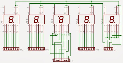
The Digital Clock Display
Fig 4: Display arrangement
Fig 5: Schematic of the Display System
For a more comprehensive and a vivid display, I decided to use LED display connected as a common-cathode 7-segment display. For those that may prefer to design the Digital clock Display using LED display, the Clock LED Display PCB shown in figure 6 will provide the needed assistance.
Fig 6: Clock LED Display PCB
Results
See figure 7 for the clock display outputs on an LED display. For a visualization of the real time operation of the digital clock design, watch media 1.
Fig 7i: Clock time in AM
Fig 7ii: Clock time in PM
Media 1: The Clock in action
Conclusion
The design goal was achieved with the time being displayed in a spectacular form on an LED display. It is worth trying out!
Related post
Related post


Please continue to write more because it’s unusual that someone has something interesting to say about this.
ReplyDeleteWill be waiting for more! To get new information visit here
bundy clocks
electronic bundy clocks
bundy cards
AVisit digital clock.com! is simple and easy to read, showing the time clearly with numbers. It’s a handy choice for any room and often comes with useful features like alarms or date displays.
ReplyDelete